How Nanowires Work

By: Jonathan Strickland  | 
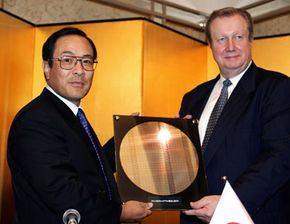
Toshiba shows off a prototype of a 90-nanometer silicon wafer. See more nanotechnology images.
Yoshikazu Tsuno/ AFP/Getty Images

In 1965, engineer Gordon Moore predicted that the number of transistors on an integrated circuit -- a precursor to the microprocessor -- would double approximately every two years. Today, we call this prediction Moore's Law, though it's not really a scientific law at all. Moore's Law is more of a self-fulfilling prophecy about the computer industry. Microprocessor manufacturers strive to meet the prediction, because if they don't, their competitors will [source: Intel].

Nanotechnology Image Gallery

Advertisement

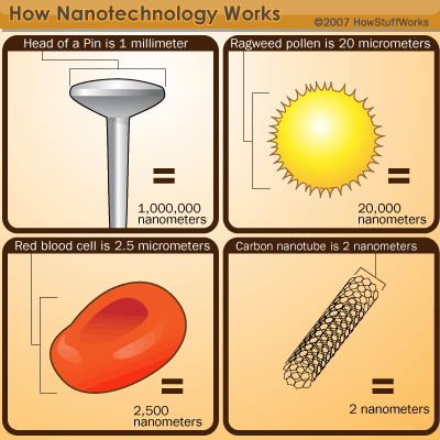
To fit more transistors on a chip, engineers have to design smaller transistors. The first chip had about 2,200 transistors on it. Today, hundreds of millions of transistors can fit on a single microprocessor chip. Even so, companies are determined to create increasingly tiny transistors, cramming more into smaller chips. There are already computer chips that have nanoscale transistors (the nanoscale is between 1 and 100 nanometers -- a nanometer is one billionth of a meter). Future transistors will have to be even smaller.

Enter the nanowire, a structure that has an amazing length-to-width ratio. Nanowires can be incredibly thin -- it's possible to create a nanowire with the diameter of just one nanometer, though engineers and scientists tend to work with nanowires that are between 30 and 60 nanometers wide. Scientists hope that we will soon be able to use nanowires to create the smallest transistors yet, though there are some pretty tough obstacles in the way.

In this article, we'll look at the properties of nanowires. We'll learn how engineers build nanowires and the progress they've made toward creating electronic chips using nanowire transistors. In the last section, we'll look at some of the potential applications for nanowires, including some medical uses.

In the next section, we'll examine the properties of nanowires.


­

Advertisement

Nanowire Properties

2007 HowStuffWorks

Depending on what it's made from, a nanowire can have the properties of an insulator, a semiconductor or a metal. Insulators won't carry an electric charge, while metals carry electric charges very well. Semiconductors fall between the two, carrying a charge under the right conditions. By arranging semiconductor wires in the proper configuration, engineers can create transistors, which either acts as a switch or an amplifier.

Some interesting -- and counterintuitive -- properties nanowires possess are due to the small scale. When you work with objects that are at the nanoscale or smaller, you begin to enter the realm of quantum mechanics. Quantum mechanics can be confusing even to experts in the field, and very often it defies classical physics (also known as Newtonian physics).

Advertisement

For example, normally an electron can't pass through an insulator. If the insulator is thin enough, though, the electron can pass from one side of the insulator to the other. It's called electron tunneling, but the name doesn't really give you an idea of how weird this process can be. The electron passes from one side of the insulator to the other without actually penetrating the insulator itself or occupying the space inside the insulator. You might say it teleports from one side to the other. You can prevent electron tunneling by using thicker layers of insulator since electrons can only travel across very small distances.

Another interesting property is that some nanowires are ballistic conductors. In normal conductors, electrons collide with the atoms in the conductor material. This slows down the electrons as they travel and creates heat as a byproduct. In ballistic conductors, the electrons can travel through the conductor without collisions. Nanowires could conduct electricity efficiently without the byproduct of intense heat.

At the nanoscale, elements can display very different properties than what we've come to expect. For example, in bulk, gold has a melting point of more than 1,000 degrees Celsius. By reducing bulk gold to the size of nanoparticles, you decrease its melting point, because when you reduce any particle to the nanoscale, there's a significant increase in the surface-to-volume ratio. Also, at the nanoscale, gold behaves like a semiconductor, but in bulk form it's a conductor.

Other elements behave strangely at the nanoscale as well. In bulk, aluminum isn't magnetic, but very small clusters of aluminum atoms are magnetic. The elemental properties we're familiar with in our everyday experience -- and the ways we expect them to behave -- may not apply when we reduce those elements down to the size of a nanometer.

We're still learning about the different properties of various elements at the nanoscale. Some elements, like silicon, don't change much at the nanoscale level. This makes them ideal for transistors and other applications. Others are still mysterious, and may display properties that we can't predict right now.

In the next section, we'll find out how engineers make nanowires.

Advertisement

Building Nanowires from the Top Down

Fiber-optic cables
David Ritter, SXC

Nanoscience specialists talk about two different approaches to building things in the nanoscale: the top-down approach and the bottom-up approach. A top-down approach essentially means that you take a bulk amount of the material you plan on using for nanowires and carve away until you are down to the right size. A bottom-up approach is an assembly process where smaller particles join to make a larger structure.

Although we can build nanowires using either approach, no one has found a way to make mass production feasible. Right now, scientists and engineers would have to spend a lot of time to make a fraction of the number of nanowires they would need for a microprocessor chip. An even greater challenge is finding a way to arrange the nanowires properly once they are built. The small scales make it very difficult to build transistors automatically -- right now, engineers usually manipulate wires into place with tools while observing everything through a powerful microscope.

Advertisement

An example of a top-down approach is the way scientists make fiber-optic nanowires. Fiber-optic wires carry information in the form of light. To make a fiber-optic nanowire, engineers first start with a regular fiber-optic cable. There are a few different approaches to reduce a fiber-optic cable to the nanoscale. Scientists could heat up a rod made out of sapphire, wrap the cable around the rod, and pull the cable, stretching it thin to create a nanowire. Another method uses a tiny furnace made from a small cylinder of sapphire. Scientists draw the fiber-optic cable through the furnace and stretch it into a thin nanowire. A third procedure called flame brushing uses a flame under the fiber-optic cable while scientists stretch it [source: Gilberto Brambilla and Fei Xu].

In the next section, we'll look at the ways scientists can grow nanowires from the bottom up.

Advertisement

Growing Nanowires

Chemical vapor deposition (CVD) is an example of a bottom-up approach. In general, CVD refers to a group of processes where solids form out of a gaseous phase. Scientists deposit catalysts (such as gold nanoparticles) on a base, called a substrate. The catalysts act as an attraction site for nanowire formation. Scientists put the substrate in a chamber with a gas containing the appropriate element, such as silicon, and the atoms in the gas do all the work. First, atoms in the gas attach to atoms in the catalysts, then additional gas atoms attach to those atoms, and so on, creating a chain or wire. In other words, the nanowires assemble themselves.

A new way to build nanowires is to print them directly to the appropriate substrate. A team of researchers in Zurich pioneered this method. First, they carved a silicon wafer so that the raised portions on the wafer coincided with the way they wanted the nanowires arranged. They used the wafer like a stamp, pressing it against a synthetic rubber called PDMS. They then drew a liquid filled with gold nanoparticles, called a colloidal suspension, across the PDMS. The gold particles settled into the channels created by the silicon wafer stamp. Now the PDMS became a mold capable of transferring a "print" of gold nanowires onto another surface. PDMS molds can be used repeatedly and may play a role in the mass production of nanowire circuitry in the future [source: Nature Nanotechnology].

Advertisement

Several laboratories have created transistors using nanowires, but their creation requires a lot of time and manpower. Nanowire transistors perform as well or better than current transistors. If scientists can find a way to design a way to produce and connect nanowire transistors together efficiently, it will pave the way to smaller, faster microprocessors, which will allow the computer industry to keep up with Moore's Law. Computer chips will continue to get smaller and more powerful.

Research in nanowire production continues across the world. Many scientists believe it's just a matter of time before someone comes up with a viable way to mass produce nanowires and nanowire transistors. Hopefully, if and when we reach that point, we'll also have a way to arrange nanowires the way we want so that we can use them to their full potential.

In the next section, we'll learn about the potential applications of nanowire technology.­

Advertisement

Nanowire Applications

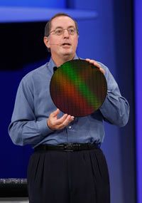
Intel CEO Paul Ortelli holds a wafer of computer chips with 32-nanometer circuitry.
Justin Sullivan/Getty Images

Perhaps the most obvious use for nanowires is in electronics. Some nanowires are very good conductors or semiconductors, and their miniscule size means that manufacturers could fit millions more transistors on a single microprocessor. As a result, computer speed would increase dramatically.

Nanowires may play an important role in the field of quantum computers. A team of researchers in the Netherlands created nanowires out of indium arsenide and attached them to aluminum electrodes. At temperatures near absolute zero, aluminum becomes a superconductor, meaning it can conduct electricity without any resistance. The nanowires also became superconductors due to the proximity effect. The researchers could control the superconductivity of the nanowires by running various voltages through the substrate under the wires [source: New Scientist].

Advertisement

Nanowires may also play an important role in nano-size devices like nanorobots. Doctors could use the nanorobots to treat diseases like cancer. Some nanorobot designs have onboard power systems, which would require structures like nanowires to generate and conduct power.

Using piezoelectric material, nanoscientists could create nanowires that generate electricity from kinetic energy. The piezoelectric effect is a phenomenon certain materials exhibit -- when you apply physical force to a piezoelectric material, it emits an electric charge. If you apply an electric charge to this same material, it vibrates. Piezoelectric nanowires might provide power to nano-size systems in the future, though at present there are no practical applications.

There are hundreds of other potential nanowire applications in electronics. Researchers in Japan are working on atomic switches that might some day replace semiconductor switches in electronic devices. Scientists with the National Renewable Energy Laboratory hope that coaxial nanowires will improve the energy efficiency of solar cells. Because we are still learning about the properties of nanowires and other nanoscale structures, there could be thousands of applications we haven't even considered yet.

To learn more about nanowires and related topics, follow the links on the next page.

Advertisement

Frequently Answered Questions

What is a nano cable?
A nano cable is a very small cable that is used to connect electronic devices. Nano cables are much smaller than regular cables, and they are often used in applications where space is limited.

Lots More Information

Related HowStuffWorks Articles

More Great Links

  • "A Nanowire with a Surprise." Brookhaven National Laboratory. October 18, 2004. http://www.bnl.gov/bnlweb/pubaf/pr/PR_display.asp?prID=04-92
  • "Chemical Vapour Deposition (CVD) - An Introduction." Azom.com. http://www.azom.com/details.asp?ArticleID=1552
  • "Moore's Law." Intel. http://www.intel.com/technology/mooreslaw/index.htm
  • "Nanoscale 'Coaxial Cables' for Solar Energy Harvesting." Physorg.com. April 23, 2007. http://www.physorg.com/news96557368.html
  • "nanotechnology." Encyclopædia Britannica. 2007. Encyclopædia Britannica Online. 11 Oct. 2007 http://search.eb.com/eb/article-9384821
  • "Nanowire Coating for Bone Implants, Stents." ScienceDaily. August 28, 2007. http://www.sciencedaily.com/releases/2007/08/070824173341.htm
  • "Nanowires form atomic switch." Nanotechweb.org. January 6, 2005. http://nanotechweb.org/cws/article/tech/21176
  • "Nanowires may provide innards for quantum computers." New Scientist. July 16, 2005. Issue 2508. Page 18.
  • "Nanowires within nanowires." Physicsworld.com. November 8, 2002. http://physicsworld.com/cws/article/news/16393
  • "Quantum Dot Introduction." Evident Technologies. http://www.evidenttech.com/qdot-definition/quantum-dot-introduction.php
  • "Scientists Turn DNA into Nanowires." Scientific American.com. January 6, 2004. http://www.sciam.com/article.cfm?articleID=00065BDA-E97C-1FF9-A97C83414B7F0144
  • "Using Nanowires to Generate Electricity by Harvesting Energy from the Environment." Azonano.com. September 28, 2007. http://www.azonano.com/news.asp?newsID=5036
  • Brambilla, Gilberto and Xu, Fei. "Optical Fibre Nanowires and Related Structures." Optoelectronics Research Centre, University of Southampton.
  • Brown, Chappell. "Bacteria grow conductive wires." EE Times. August 8, 2005. http://www.eetimes.com/showArticle.jhtml?articleID=167101011
  • Chang, Kenneth. "Nanowires May Lead to Superfast Computer Chips." The New York Times. November 9, 2001. http://query.nytimes.com/gst/fullpage.html?res=9D06E4DF1638F93AA35752C1A9679C8B63
  • Choi, Charles Q. "Nanowires common in bacteria?" The Scientist. July 11, 2006. http://www.the-scientist.com/news/display/23924/
  • Cortie, Michael B. "The Weird World of Nanoscale Gold." Gold Bulletin. Vol 37, 2004.
  • Cui, Yi. "Nanowires and Nanocrystals for Nanotechnology." Lecture at Stanford University. September 12, 2006. http://video.google.com/videoplay?docid=6571968052542741458
  • Edwards, John. "Nanowires Get Bent Out Of Shape For New Technology." Electronic Design. August 2, 2007.
  • Friedrich, Craig. "Laser Ablation." Michigan Technology University. http://www.me.mtu.edu/~microweb/chap4/ch4-2.htm
  • Gelblum, Amit. "Self-Assembling Nanowires." The Future of Things. September 26, 2007. http://www.tfot.info/news/1010/self-assembling-nanowires.html
  • Himpsel, Franz J. "Fabrication of Nanowires at Surfaces." University of Wisconsin Madison. http://uw.physics.wisc.edu/~himpsel/wires.html
  • Hoekenga, B. Christine. "Novel Nanowires for Faster Memory." MIT Technology Review. September 27, 2007. http://www.technologyreview.com/Nanotech/19428/
  • Inman, Mason. "Bacteria made to sprout conducting nanowires." NewScientist.com. July 11, 2006. http://technology.newscientist.com/article/dn9526
  • Stormer, Horst. "Small Wonders - The World of Nanoscience." Lecture. November 14, 2006. http://video.google.com/videoplay?docid=8197935869304489599
  • Timmer, John. "Nanoscale printing: better nanowires through 100,000 dpi printing." Ars Technica. September 11, 2007. http://arstechnica.com/news.ars/post/20070911-nanoscale-printing-better-nanowires-through-100000-dpi-printing.html
  • Yarris, Lynn. "Embedded: A Benign Way to Nanowire Living Cells." Science@Berkeley Lab. August 6, 2007. http://www.lbl.gov/Science-Articles/Archive/sabl/2007/Jul/embedded.html

Advertisement

Loading...